
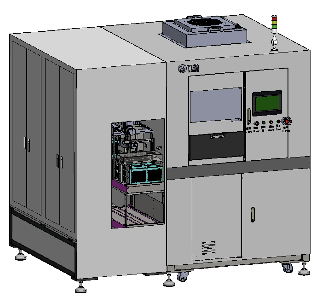
HW CS5025
Brand: Symphony AOI
Applied in post-encapsulation or post-plating processes, it can detect the defects in the chip surface and pin, improving efficiency and yield.
|
Project |
Content |
|
Application Scenarios |
Both front and back sides of the strip and substrate are inspected |
|
Applicable Product Specifications |
Width: 40X100mm, length: 100x300mm |
|
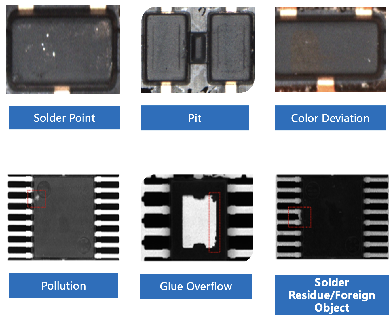
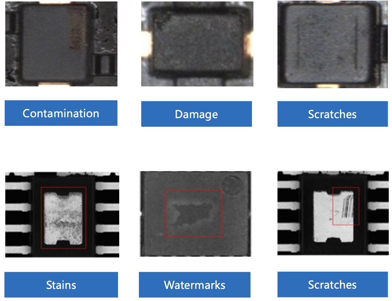
Identifiable Defect Types |
Scratches, foreign objects, contamination, copper leakage, pressure damage, glue overflow, bubbles, damage, pits, discoloration, deformation, etc |
|
Imaging System |
Line scan camera, area array camera, laser profiler |
|
Cassette and Transmission Mode |
Left-in-left-out |
|
Lens and Resolution |
2500W color |
|
Accuarcy |
5um/pixel |
|
Optional and Designated |
Inkjet marking or laser marking |