
Product Brands
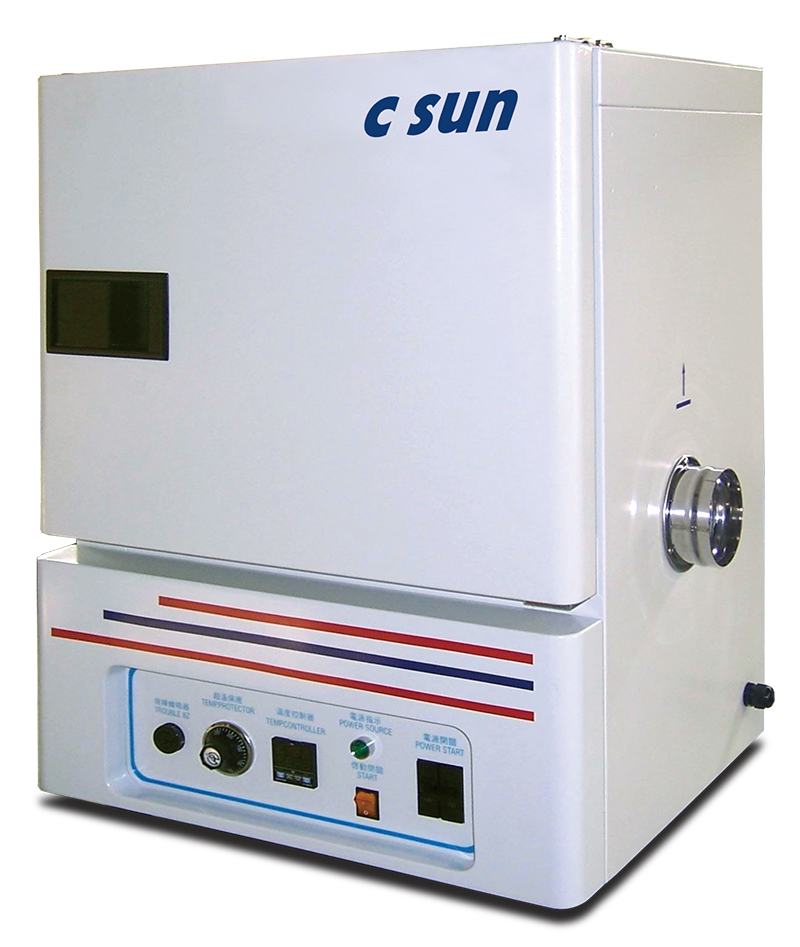
Leader in Thermal and UV Light Process Equipment since 1966
Discover HORIBA’s advanced particle size analyzers, zeta potential analyzers, and nanoparticle characterization systems, supplied by Symphony Engineering – the authorized distributor and trusted supplier in Malaysia. Our solutions support R&D and quality control (QC) across industries including pharmaceuticals, chemicals, semiconductors, electronics, and nanotechnology.
Advance your research with Thermo Scientific FTIR, Raman, infrared microscopy, and gas analysis instruments, supplied by Symphony Engineering – the exclusive distributor in Malaysia. These systems deliver industry-leading accuracy and ISO-compliant results, supporting failure analysis, molecular science, and industrial quality control (QC). Trusted across pharmaceuticals, semiconductors, polymers, chemicals, and nanotechnology, Thermo Scientific spectroscopy solutions empower laboratories in Malaysia to solve complex material challenges with confidence.
Precision Machining & Custom Parts Fabrication for OEM and Engineering Projects
Accredited Calibration for Dimensional, Electrical and Temperature
Automation and Robotics
Automatic Optical Inspection (AOI)
Precision Machining in Semiconductor Advanced Packaging
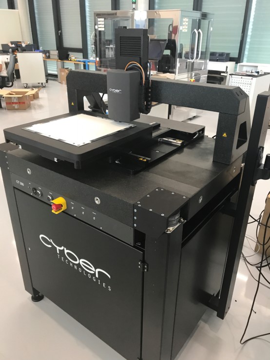
High End 3D CT X-Ray
Microscopy Solution - More than Microscopy
Scanning Acoustic Microscopy Analytical Systems
Auto and Accurate Bond Tester
Laser Range Finder
Wafer Inspection Systems
Reflow Simulator for Observation and Measurement
High Resolution 3D Surface Non-Contact Measurement Systems
Nikon XTV160 Xray
Microwave Plasma Decapsulation System
eviXscan 3D is a brand of high quality scanners based on structured light technology
Electron Microscope Supplies
Full solution of Metallography, Metallurgical Testing, Microstructural Analysis
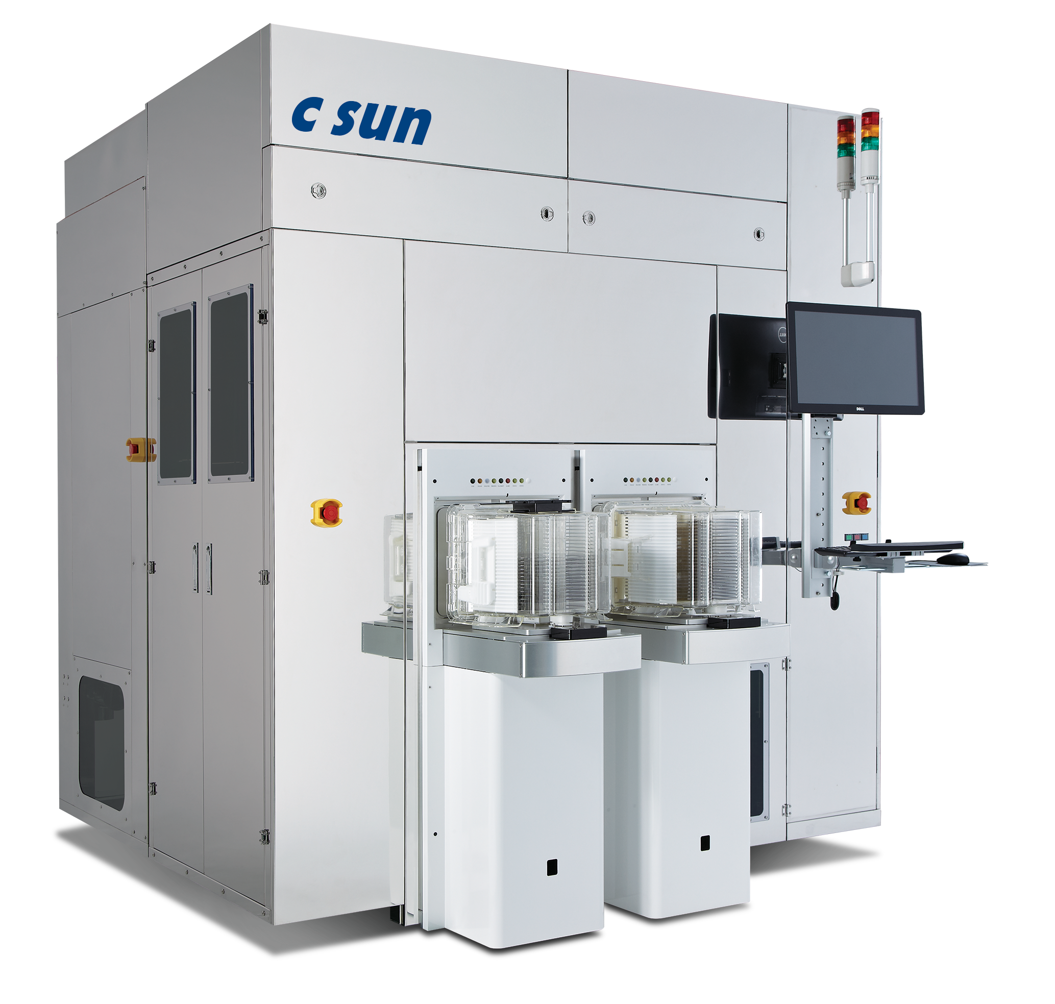
Leader in Wafer AOI and Precision Grinding in Semiconductor Advanced Packaging
- Brand
- Symphony Automation
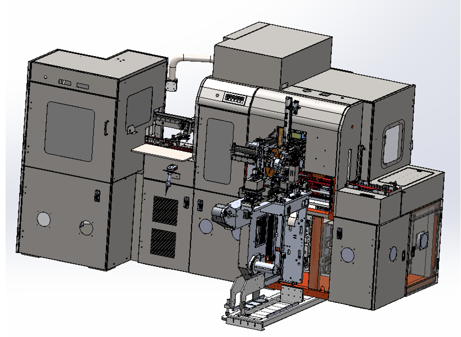
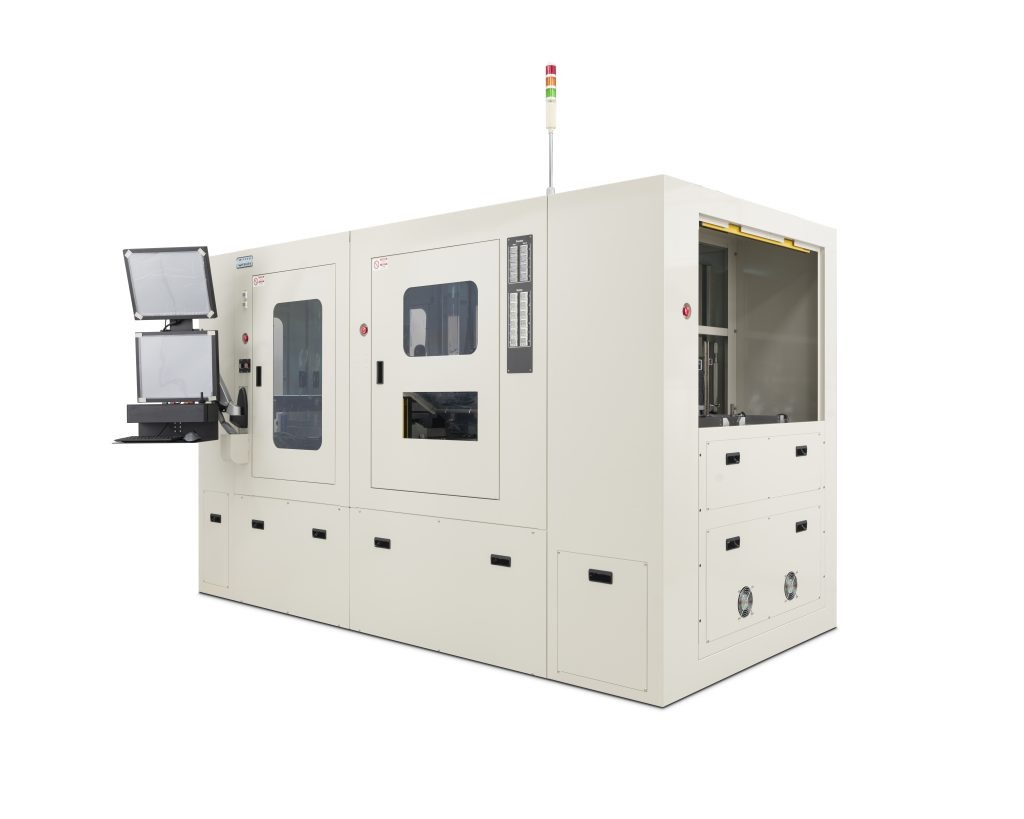
Symphony Smart Auto Reel Changer
High-speed, fully automated reel changing system with intelligent sensing and minimal manual intervention - Ideal for SMT and semiconductor packaging lines to enhance efficiency and reduce downtime.
- Brand
- Symphony AOI
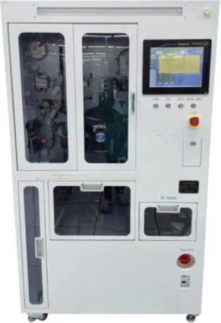
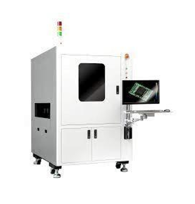
HW 5010TR and HW 5010TT
Applied after final test, it can detect appearance defects in encapsulated devices by patented 2D/3D vision inspection system.
- Brand
- Symphony AOI
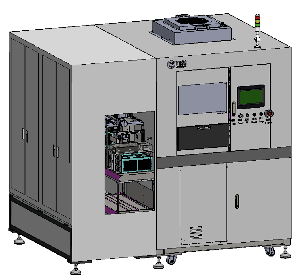
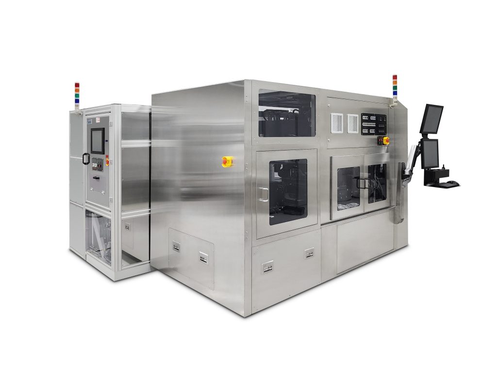
HW CS5025
Applied in post-encapsulation or post-plating processes, it can detect the defects in the chip surface and pin, improving efficiency and yield.
- Brand
- Symphony AOI
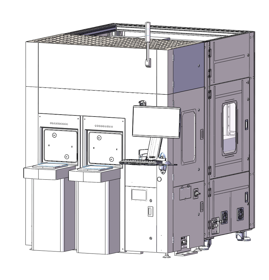
HW Wafer AOI 5510
Applied to shipment after wafer cutting/post-seal cutting, it detects um-level defects on 6-12 inch wafers, provides yield feedback and outputs map to optimize efficiency
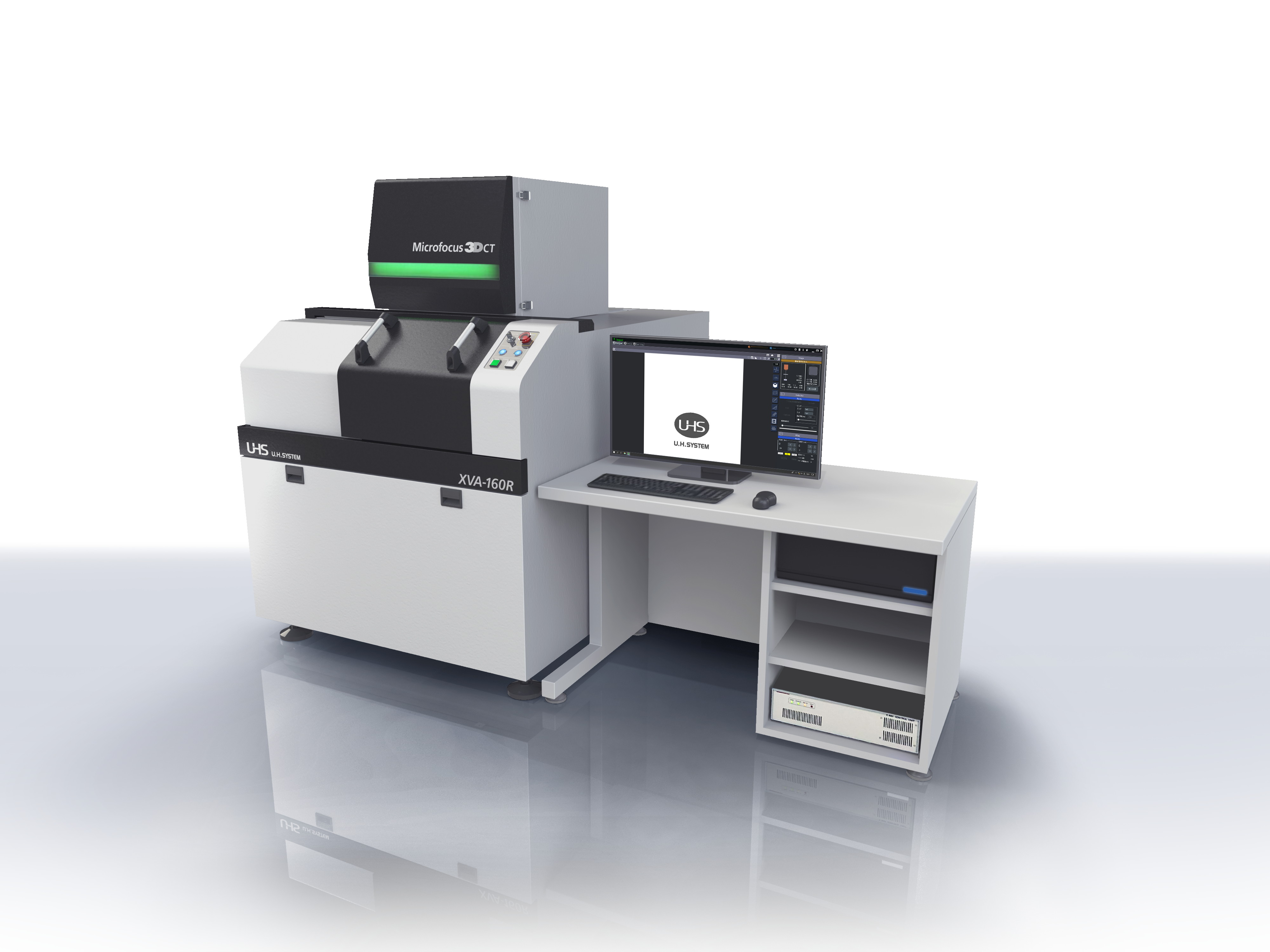
- Brand
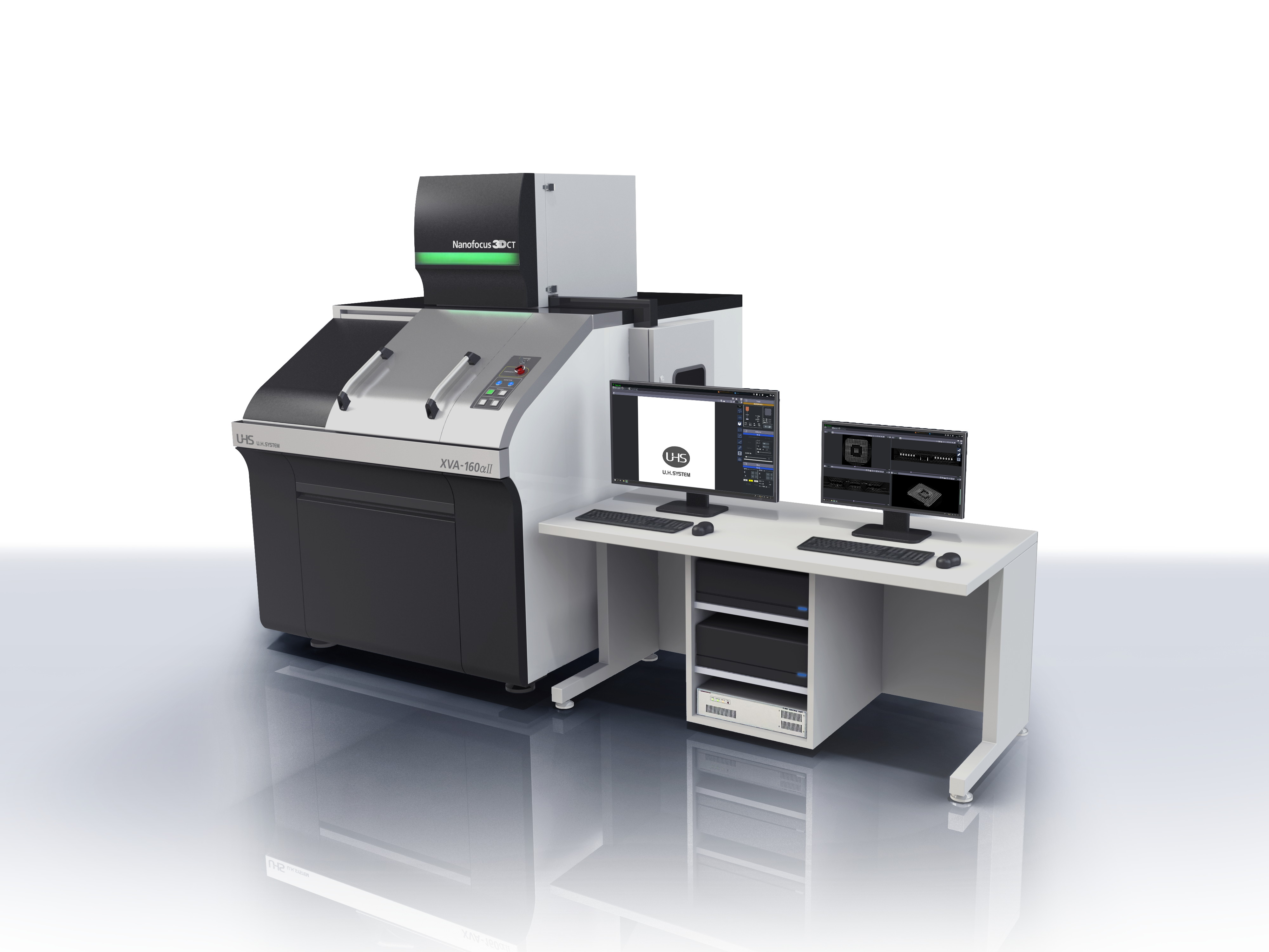
- UHS 3D CT Xray
XVA 160 Alpha II Z
3D X-ray CT system High-end Nano-focus model, ideal for inspection & analysis of semiconductors & electronic components.
- Brand
- UHS 3D CT Xray
XVA 160RZ
High resolution 3D X-ray CT system Versatile MicroFocus model, perfect for inspection & analysis of SMT boards or other items.
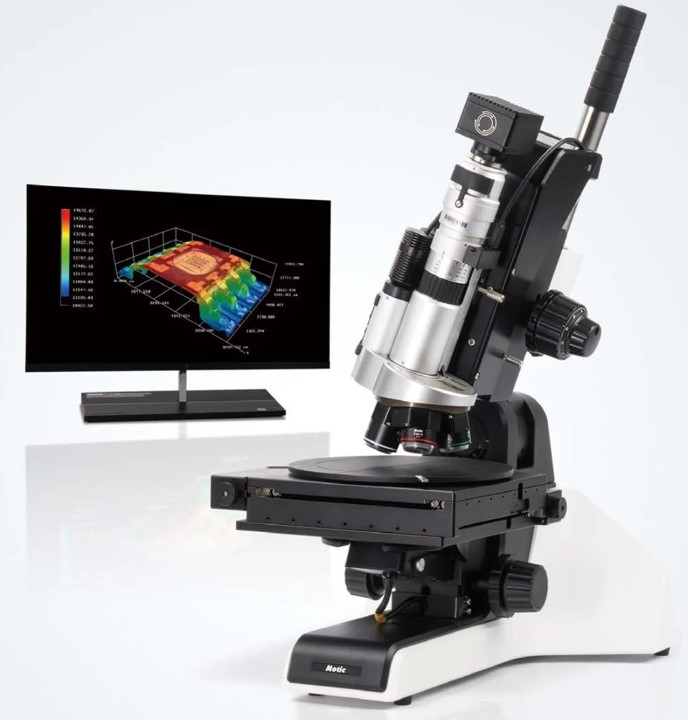
- Brand
- Motic
Easy Zoom Digital Microscope
A flexible, high performance digital microscope that is well suited for material inspection. The microscope offers 50x to 5800x magnification in a single zoom body, providing extreme versatility and making it a great fit for any application.