
cyberTECHNOLOGIES for Semiconductor Application
Application: Semiconductor & Electronics
High-resolution, non-contact 3D measurement system options to the microelectronics
CYBERTECHNOLOGIES CT300 - VIEW PRODUCT
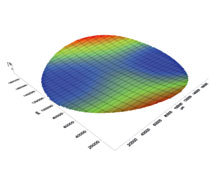 TTV
TTV
Surface of a silicone wafer
- Accurate flatness measurement over large areas
- Colors can be set to specification limits
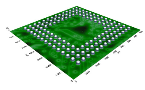
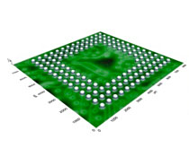 Coplanarity
Surface image of a Micro BGA
- Measure max. height, diameter and position of each bump
- Regression and seating plane coplanarity
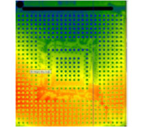 Flatness
Countour map of an electronic component
- Advanced etch removing and modifiying algorithms
- Use polygon shape cursors to mark region of interest