
EBIS Wafer Backside Optical Inspection
Brand: PVA TePla SPA
Semi-automatic Wafer Backside Inspection System
YOUR BENEFITS
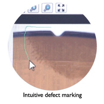
- Semi-automatic macroscopic defect detection on wafer backside
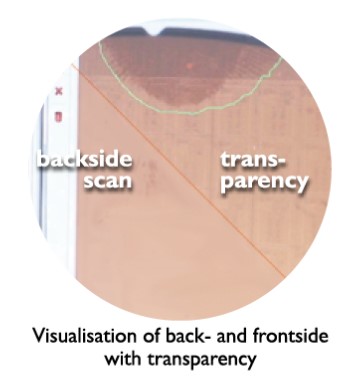
- Visualization of complete wafer backside on the screen
- Transparent wafer frontside overlay during backside defect marking
- Automatic wafermap edit when backside defect is marked
- Fast automatic loading and scanning process (up to 250 wph)
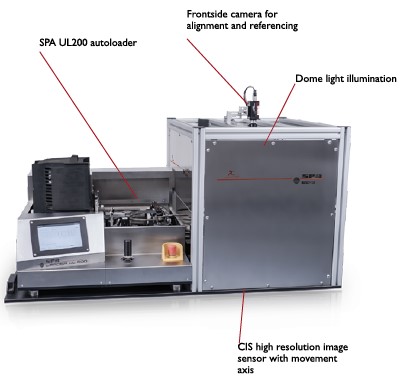
TECHNICAL COMPONENTS
- SPA ULA200 Autoloader
- CIS High Resolution Image Sensor with movement axis
- Dome Light Illumination
- Frontside Camera for Alignment and Referencing
TECHNICAL SPECIFICATIONS
- Wafer diameter up to 200mm (300mm on request)
- Thin and Taiko wafer on request
- Backside scan resolution down to 21um/px
- Optional SECS/GEM Compatible Interface
- Various adaptable wafermapping formats