
Semi Automatic Wafer Inspection
Brand: PVA TePla SPA
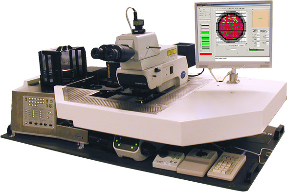
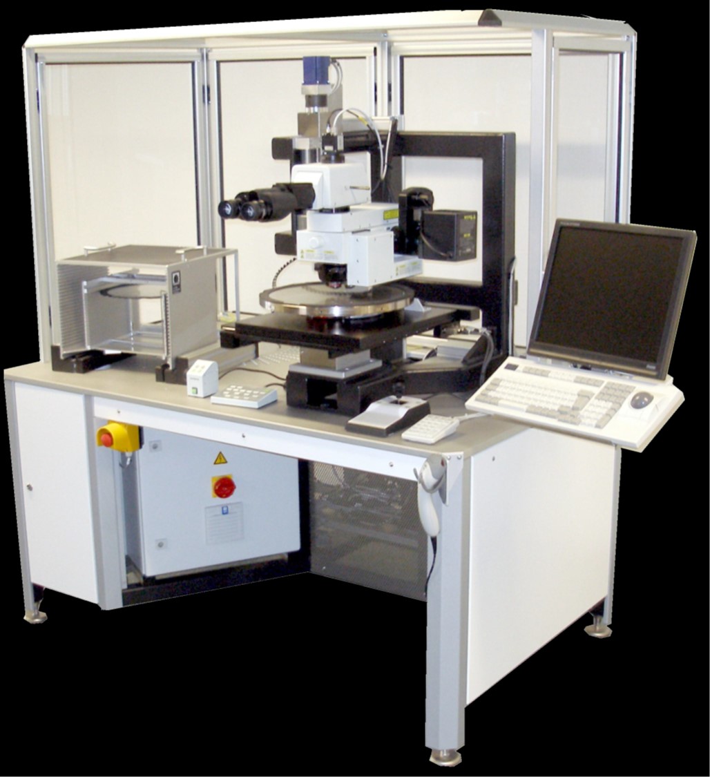
Wafer Inspection System with Wafer Loader and Wafer Mapping Software
Tabletop solutions
– Various Microscope models
– Automatic SPA UL200 wafer loader
– High speed / precision stage
– OCR / barcode wafer identification
– Top/back macro (with illumination)
– Micro inspection (automatic chip positioning)
– Map import/export function (TSK, EG, TEL, SPAwn)
– Vision system for automatic wafer alignment
– Image acquisition and database storage
– High resolution- or high speed camera appliable
100% wafer or sample chip inspection
– 4 to 8 inch wafer capability
– handles more than 500000 dies / wafer
– various sample die inspections (AQL, LTPD, ..)
– Wafer edge die inspection
– gross defect inspection (scratches)
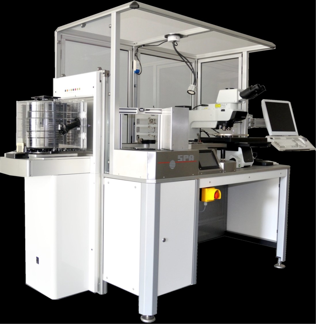
200 – 300mm wafer bridge tool (Diced Wafer option available with Wafer Frame Loading)
– Isel Robotics wafer handling
– Various Microscope models
– SPA UL loader touchscreen interface
– High speed / precision stage
– OCR / barcode wafer identification
– Top/back macro (with illumination)
– Micro inspection (automatic chip positioning)
– Map import/export function (TSK, EG, TEL, ..)
– Vision system for automatic wafer alignment
– Image acquisition and database storage
– High resolution- or high speed camera appliable
100% wafer or sample chip inspection
– 8 - 12 inch wafer capability
– 8 inch Taiko/thin wafer
– handles more than 500000 dies / wafer
– various sample die inspections (AQL, LTPD, ..)
– Wafer edge die inspection
– gross defect inspection (scratches)
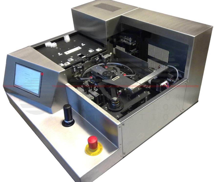
Optional automatic inspections
– probe mark inspection
– defect inspection (eg. CD – critical dimensions)