
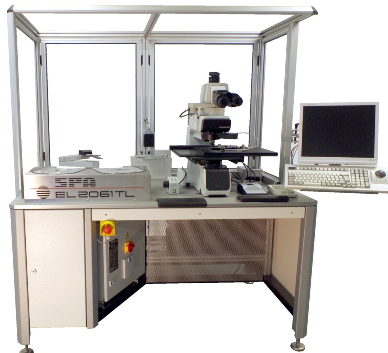
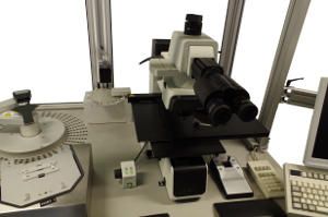
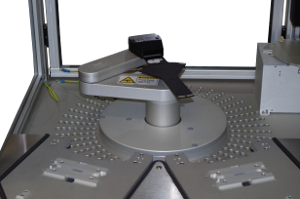
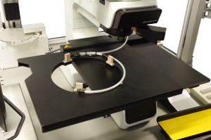
SPA Inspector IR Wafer Inspection
Brand: PVA TePla SPA
AOI of Wafer Surfaces and Layers in 2D with IR Technology
IR Inspector Basics
- Microscope inspection 6" and 8" wafer
- Edge wafer handling
- Throughlight for IR inspection
- Fully automatic process
- ID Reader (via ethernet I/F)
- Map reading, updating, creating
- Chip inspection 100% or in sample mode
IR Inspector Options
- Various network adaptions
- SECSII/GEM interface
- Upgrade for 12" wafers
- Online/Offline manual review of defects
- Open architecture for future add ons
Inspection Features
- Pattern measurement within wafer layers
- Critical Dimension (CD) measurement
- Pattern offset measurement (top to bottom layer)
- Customer specific project developements